


(Reprinted by permission of LSI Logic Corporation)
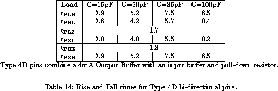
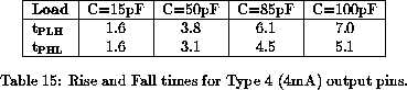
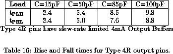
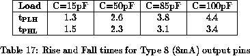
The CMOS output drivers used in the PCL are strongly affected by capacitative load. Tables 14,15,16 and 17 give the effect of different loads on output rise and fall times.
The output pins do not have sufficient output current capability to drive a terminated line. It is recommended that the maximum trace length connected to an output pin be limited such that twice the signal transmission time of the trace does not significantly exceed the rise time of the signal, in order to avoid ringing.