Three external timing elements are used by the PCL to time all operations:
IST is connected to OST
via a short delay of
about 5ns (1.0k
and
stray capacitance). The delay in the pin I/O drivers is the significant
part of this delay. It is used for strobing internal latches and
compensating for internal delays. This delay must be fairly symmetrical
as both rising and falling edges are used.
ILT is connected to OLT
via a
longer delay which is used to
compensate for parity generation and SS code generation delays and also
for Write and Read access time to user registers. It should be set at
the greater of the worst write or read access time for any user
register, or 90ns. Both rising and falling edge delays are used. An RC
integrator or similar delay device should be used. The maximum delay
should be less than 1 microsecond; slower devices should use Busy
(IBSY)
or
the WT line. If an RC network is used, low-bias diodes may be used to give
separate adjustment of the rise and fall times. The rise time may then be
reduced where parity
has been disabled.
IUAT is connected to OUAT
via a delay equal to that
between the NTA
increment signal and stabilized access to any user
register. This includes NTA clock to OACA/OACB
(max 50ns),
the user's NTA decoder delay and the address access time of the user's
registers. It does not have to include the read access time for the user's
registers, which is compensated for by the long timer.
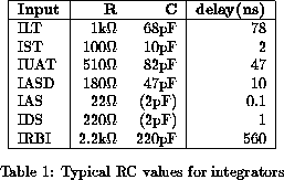
Table 1 gives typical values for the integrator components. These
figures are guidelines only, based on the prototype performance. Delays in user
designs must be tuned for correct operation and optimal performance.
The figure 2pF shown in brackets refers to the input pin capacitance; no
external capacitor is required.