


Logic has been included in the PCL to enable Multiblock operation - see Appendix A for the Multiblock specification. It was not feasible to include complete Multiblock logic inside the PCL gate array since considerations of cost and package size limited the number of pins available, so external logic is required to achieve Multiblock functionality.
A group of modules connected for Multiblock operation consists of a Primary module, zero or more Middle modules and an End module. The PCL input IFAT is used in the following manner:
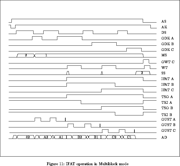
Data transfer from the Primary module proceeds in the normal fashion (the PCL asserting AK, DK and OUST) until the end of data in the Primary module. The external logic then asserts WT, drives IFAT high and initiates a handshake to the adjacent Middle or End module. The high level on IFAT causes the attached PCL to enter a quiescent state; it continues to assert AK but no longer asserts DK or OUST. The timers, however, continue to run since a subsequent secondary address cycle may return control to the Primary module.
When control is passed to a Middle or End module, the external logic drives
IFAT high. A high level on IFAT while AK is high causes an
unattached PCL to be activated; it runs timing cycles, asserts DK and OUST,
and behaves as if it were attached (though it does not assert AK). When the
end of data in a Middle or End module is reached, the external logic drops
IFAT which causes the PCL to resume a true disconnected state, (and if a
Middle module, initiates a handshake to the next module).
When AS falls the primary PCL asserts OWT until all the middle and
end modules have properly detached.
Figure 11 shows the relevant waveforms.
The following ABEL file implements the Multiblock logic for the PCL in 3
PALs. The logic may be substantially simplified if advanced mode is not used;
it may be possible to use the OSA signal instead of IRD and IMS(2:0).
Figure 12 on page  gives the relevant schematic.
module mbglue
title 'Logic for Multiblock operation using PCL'

" Caution: This logic has been simulated but not tested; correct operation
" is not guaranteed.

    PLA1 device 'P22V10' ;
    PLA2 device 'P20RA10' ;
    PLA3 device 'P22V10' ;

" This design needs asynchronous flipflops, which are in the 20RA10.
" The 22V10s are used in combinatorial mode; any device with sufficient
" product terms and pins could be used.

" IADV=0 if IADV to PCL is tied low, else 1
    IADV = 1 ;

" PLA1 inputs
    MBA_FB pin in PLA1 1 "I0" ;             " monostable feedback
    IMS0,IMS1,IMS2,IRD pin in PLA1 2,3,4,5 "I(1:4)" ; " from segment transceivers
    IAS,IAK pin in PLA1 6,8 "I5,I7" ;       " from segment transceivers
    ONCL pin in PLA1 7 "I6" ;               " from PCL; Clear signal
    OST,OLT pin in PLA1 9,10 "I8,I9" ;      " from PCL timers
    OLTD pin in PLA1 11 "I10" ;             " OLT delayed by 50ns (RC network)
    TSI pin in PLA1 13 "I11" ;              " from daisychain transceivers
    MBC0,MBC1 pin in PLA1 15,14 "IO9,IO10" ; " multiblock control bits (from CSR#0)
    FIFO_ERR pin in PLA1 16 "IO8" ;         " from FIFO indicating it is
                                            " FULL (for a write cycle)
                                            " or EMPTY (for a read cycle)
    IFAT pin in PLA1 17 "IO7" ;             " from PLA2

" PLA1 outputs
    NTAWT_RE pin in PLA1 18 "IO6" ='pos' ;  " to PLA2
    NTAWT_PR pin in PLA1 19 "IO5" ='pos' ;  " to PLA2
    HANDOVER pin in PLA1 20 "IO4" ='pos' ;  " Signals that hand-over to next
                                            " module should occur

    MBSTOP pin in PLA1 21 "IO3" ='pos' ;    " indicates that multiblock
                                            " operation should stop.
    MBCYC pin in PLA1 22 "IO2" ='pos' ;     " to PLA2, PLA3 - timing signal
    MB_ACCESS pin in PLA1 23 "IO1" ='pos' ; " MB active to LED (monostable)
" PLA2 inputs
    VCC pin in PLA2 1 "PL~" ;               " preload pin (tied high)
    MBCYC pin in PLA2 2 "I0" ;              " from PLA1
    MBSTOP,HANDOVER pin in PLA2 3,4 "I1,I2" ; " from PLA1
    NTAWT_PR,NTAWT_RE pin in PLA2 5,6 "I3,I4" ; " from PLA1
    DSR2 pin in PLA2 7 "I5" ;               " Dataspace location 2 select
                                            " (from address decoder)
    MBC0,MBC1 pin in PLA2 8,9 "I6,I7" ;     " multiblock control bits (from CSR#0)
    TSI pin in PLA2 10 "I8" ;               " from daisychain transceivers
    OST pin in PLA2 11 "I9" ;               " short timer from PCL
    ENTS pin in PLA2 15 "O8" ;              " from PLA3
    MBERR_PR pin in PLA2 20 "O3" ;          " from PLA3
    IFAT_PR,IFAT_RE pin in PLA2 22,21 "O1,O2" ; " from PLA3

" PLA2 outputs
    IFAT pin in PLA2 14 "O9" ='reg,pos';    " to PCL; enables data cycles
                                            " (primary) or disables (middle/end)
    NTAWT pin in PLA2 16 "O7" ='reg,pos';   " to PLA3 ; delays DK(d) for MS=6
                                            " or MS=7 NTA operaion
    MBMENRDY pin in PLA2 17 "O6" ='reg,pos';"to PLA3; middle/end not ready
    MBPDONE pin in PLA2 18 "O5" ='reg,pos'; " multiblock access of Primary
                                            " module finished ; to PLA3
    MBMDONE pin in PLA2 19 "O4" ='reg,pos'; " multiblock access of Middle
                                            " module finished ; to PLA3.
                                            " also drives IBSY on PCL to
                                            " suppress data cycle on handover
    MBERR pin in PLA2 23 "O0" ='reg,pos';   " Multiblock error to address decoder
                                            " (causes SS=3 assertion)

" PLA3 inputs
    OWT pin in PLA3 1 "I0" ;                " from PCL
    MBMDONE,MBPDONE pin in PLA3 4,5 "I3,I4" ;  " from PLA2
    MBMENRDY pin in PLA3 6 "I5" ;           " from PLA2
    NTAWT pin in PLA3 7 "I6" ;              " from PLA2
    DSR2 pin in PLA3 8 "I7" ;               " Dataspace #2 select
    MBC0,MBC1 pin in PLA3 9,10 "I8,I9"  ;   " from CSR#0
    TSI,TKI pin in PLA3 11,13 "I10,I11" ;   " from daisychain transceivers
    HANDOVER pin in PLA3 18 "IO6" ;         " from PLA1
    MBSTOP pin in PLA3 19 "IO5" ;           " from PLA1
    MBCYC pin in PLA3 20 "IO4" ;            " from PLA1
" PLA3 outputs
    ENTS pin in PLA3 14 "IO10" ='pos' ;     " to PLA2
    TSO pin in PLA3 15 "IO9" ='pos' ;       " to daisychain transceiver
    TKO pin in PLA3 16 "IO8"='pos' ;        " to daisychain transceiver
    TWT pin in PLA3 17 "IO7" ='pos' ;       " to segment WT transceiver
    MBERR_PR pin in PLA3 21 "IO3" ='pos' ;  " to PLA2
    IFAT_PR pin in PLA3 23 "IO1" ='pos' ;   " to PLA2
    IFAT_RE pin in PLA3 22 "IO2" ='pos' ;   " to PLA2

" Declarations
    IMS = [IMS2..IMS0] ; " MS code
    MBC = [MBC1..MBC0] ; " Multiblock control code
    H = 1 ; L = 0 ; Z = .X. ; X = .X. ; " assignments for test vectors

" (ABEL syntax: # means OR, & means AND, == means .EQ.)

" Macros
    MBPRI macro {(MBC==1)} ;        " Multiblock Primary module
    MBMID macro {(MBC==3)} ;        " Multiblock Middle module
    MBEND macro {(MBC==2)} ;        " Multiblock End module
    MBM_E macro {(MBMID # MBEND)} ; " Middle or end module

    NTA_OP macro {((IMS == 2) # ((IMS == 6) " NTA operation
        # (IMS == 7) & !IRD) & IADV)} ;
    MS5 macro {((IMS == 5) & IADV)} ;       " MS=5 buffer access
    MS7R macro {((IMS == 7) & IRD & IADV)} ; "MS=7 read CSR#0 operation

    MBMERUN macro {(MBM_E & TSI)} ;
    ENSS3 macro {(!TKI & !TSO)} ;           " Multiblock error (assert SS=3)
    TSPASS macro {(TSI & (MBC==0))} ;       " pass TSI
    MBACK macro {(TKI # MBEND)} ;           " acknowledge
    PTSO macro {(MBMDONE # MBPDONE # TSPASS)} ;

    MBWT macro {(TSO & TKI)} ; " asset WT during transfer
equations in PLA1

    enable HANDOVER = 1 ;
    HANDOVER = FIFO_ERR & !MS5 & !MS7R ;    " hand-over at FIFO end unless
                                            " buffer access or CSR#0 read

    enable MBSTOP = 1 ;             " stop MB if NTA operation, AS low or Clear
    MBSTOP = NTA_OP & OLT           " wait till start of cycle
         # NTA_OP & MBM_E & !IFAT   " unless an inactive mid/end module
         # !IAS # !IAK # !ONCL ;

    enable MB_ACCESS = 1 ;
    !MB_ACCESS = (IFAT & MBMERUN) # !MBA_FB ;

    enable MBCYC = 1 ;
    MBCYC = !OST & OLT & OLTD ;     " timing signal for MB logic

    enable NTAWT_PR = IADV ;
    NTAWT_PR = NTA_OP & MBPRI & IADV & IFAT ;

    enable NTAWT_RE = IADV ;
    NTAWT_RE = (!IAS # !ONCL) & IADV ;
equations in PLA3

    enable TWT = 1 ;
    TWT = OWT # MBWT # NTAWT & IADV ;  " WT on PCL or MB handover
                                        "or NTA cycle (DS(d))

    enable TSO = 1 ;
    TSO = PTSO ;

    enable TKO = 1 ;
    TKO = !(!MBACK # MBMENRDY & MBMERUN # MBPRI) ;

    enable ENTS = 1 ;
    ENTS = TKI & !TSO ;

" These set and reset terms cannot be made in PLA2 since
" the 20RA10 has only one product term for set/reset

    enable IFAT_PR = 1 ;
    IFAT_PR = MBPDONE # MBMERUN & MBACK ;          "IFAT set

    enable IFAT_RE = 1 ;
    IFAT_RE = MBSTOP # MBMERUN & !MBACK ;          "IFAT clear

    enable MBERR_PR = 1 ;
    MBERR_PR = ENSS3 & MBCYC & MBMID & HANDOVER & TSI " MBERR set
             # ENSS3 & DSR2 & HANDOVER & MBPRI ;
equations in PLA2
" swap .PR and .RE functions since 20RA10 has inverting outputs

    enable MBMENRDY = 1 ;
    MBMENRDY := MBMERUN ;
    MBMENRDY.C = !OST ;
    MBMENRDY.PR = MBSTOP ;
    MBMENRDY.RE = 0 ;

    enable MBERR = 1 ;
    MBERR.RE = MBERR_PR & !MBSTOP ;
    MBERR.PR = MBSTOP ;

    enable MBPDONE = 1 ;
    MBPDONE.RE = MBPRI & ENTS & MBCYC & DSR2 & HANDOVER & !MBSTOP ;
    MBPDONE.PR = MBSTOP ;

    enable MBMDONE = 1 ;
    MBMDONE.RE = ENTS & MBCYC & MBMID & HANDOVER & TSI & !MBSTOP ;
    MBMDONE.PR = MBSTOP ;

    enable IFAT = 1 ;
    IFAT.RE = IFAT_PR & !MBSTOP & !OST ;
    IFAT.PR = IFAT_RE ;

    enable NTAWT = IADV ;
    NTAWT:= 0 ;
    NTAWT.RE = NTAWT_PR & IADV ;
    NTAWT.PR = NTAWT_RE & IADV ;
    NTAWT.C = !OST & IADV ;    " clear NTAWT on OST(d)

"test vectors removed to save space

end mbglue
module NTA_DEC
title 'Address Decoder for Multiblock Application'

    PLA4 device 'P16P8' ;

" Inputs
    MBERR pin 1 ;       " from multiblock PLA2 (gives SS=3)
    FIFO_ERR pin 2 ;    " from FIFO indicating FULL (write) or EMPTY (read)
    OCND pin 3 ;        " from PCL (indicates CSR space selected)
    OAOR pin 4 ;        " OA wire-OR as follows:
                        " OAOR = ADI_HI:OACA w# ADI_HI:OACB w# ADI_LO:OACA
                        " w# ADI_LO:OACB w# !(OA30 # OA31) w# !(OA2 # OA3) ;
    IFAT pin 5 ;        " from multiblock PLA2 (also drives PCL)
    MBC0,MBC1 pin 6,7 ; " from CSR#0 - multiblock control bits
    ORD pin 8 ;         " from PCL
    OA1,OA0 pin 9,11 ;  " address bits (from adi)
    MBMDONE pin 13 ;    " from multiblock PLA2

" Outputs
    USS3 pin 12 ='pos' ;       " drives IUS0 and IUS1 on PCL
    ISSD pin 14 ='pos' ;       " to PCL
    FIFO_A pin 15 ='pos' ;     " selects FIFO
    DSR2 pin 16 ='pos' ;       " to multiblock PALs; dataspace register #2 selected
    IAC2,IAC1,IAC0 pin 17,18,19 ='pos' ; " address code to PCL

" Definitions
    IAC = [IAC2..IAC0] ; MBC = [MBC1..MBC0] ; OA_10 = [OA1..OA0] ;
    X=.X. ;

equations

enable USS3 = 1; enable ISSD = 1; enable FIFO_A = 1;
enable DSR2 = 1; enable IAC2 = 1; enable IAC1 = 1; enable IAC0 = 1;

ISSD= MBMDONE ;
truth_table ([MBERR,FIFO_ERR,OCND,OAOR,IFAT,MBC,OA_10] ->
    [USS3,ISSD,FIFO_A,DSR2,IAC])

  [0,X,0,1,0, X,  0] -> [0,0, 0,0, 2] ; "  DSR#0 : code 2 (error)                                         .
  [0,0,0,1,0, X,  1] -> [0,0, 1,0, 5] ; "  DSR#1 : code 5 (FIFO)
  [0,1,0,1,0, X,  1] -> [0,0, 1,0, 6] ; "  DSR#1 : code 6 (FIFO end)
  [0,X,0,1,0, 0,  2] -> [0,0, 0,0, 2] ; "  DSR#2 : code 2 (error)
                                        "   (not configured - DSR2 not MB primary)
  [0,X,0,1,0, 2,  2] -> [0,0, 0,0, 2] ; "  DSR#2 : code 2 (error)
                                        "   (end DSR2 access not MB primary)
  [0,X,0,1,0, 3,  2] -> [0,0, 0,0, 2] ; "  DSR#2 : code 2 (error)
                                        "   (middle DSR2 access not MB primary)
  [0,0,0,1,0, 1,  2] -> [0,0, 1,0, 5] ; "  DSR#2 : code 5 (FIFO) (prim link read/write)
  [0,1,0,1,0, 1,  2] -> [0,0, 1,1, 6] ; "  DSR#2 : code 6 (FIFO) (prim link EOB, transfer)
  [0,X,0,1,0, X,  3] -> [0,0, 0,0, 2] ; "  DSR#3 : code 2 (error)
  [0,X,0,0,0, X,  X] -> [0,0, 0,0, 2] ; "  bad dataspace : code 2 (error)
  [0,X,X,X,1, 1,  X] -> [0,1, 1,1, 6] ; "  multiblock access primary, transferred
  [0,0,X,X,1, 2,  X] -> [0,0, 1,0, 5] ; "  multiblock access end no error
  [0,0,X,X,1, 3,  X] -> [0,0, 1,0, 5] ; "  multiblock access end no error
  [0,1,X,X,1, 3,  X] -> [0,0, 1,1, 6] ; "  multiblock access middle EOB  , transfer
  [0,1,X,X,1, 2,  X] -> [0,0, 1,0, 6] ; "  multiblock access end EOB (SS=2)
  [0,X,1,1,0, X,  0] -> [0,0, 0,0, 0] ; "  CSR#0 : code 0
  [0,X,1,1,0, X,  1] -> [0,0, 0,0, 7] ; "  CSR#1 : code 7 (=csr#7)
  [0,X,1,1,0, X,  2] -> [0,0, 0,0, 2] ; "  CSR#2 : code 2 (error)
  [0,X,1,1,0, X,  3] -> [0,0, 0,0, 3] ; "  CSR#3 : code 3 (logical address)
  [0,X,1,0,0, X,  X] -> [0,0, 0,0, 2] ; "  bad CSR : code 2 (error)
  [1,X,X,X,X, X,  X] -> [1,1, 0,0, 2] ; "  multiblock transfer err. SS3.
"  [X,X,X,X,X, X,  X] -> [0,1, 0,0, 2] ;    make SS=0 when MB middle done

" all unimplemented locations should produce an IAC of 2
test_vectors
 ([MBERR,FIFO_ERR,OCND,OAOR,IFAT,MBC0,MBC1,OA1,OA0] ->
    [USS3,ISSD,FIFO_A,DSR2,IAC2,IAC1,IAC0])

  [0,X,0,1,0, X,X,  0,0] -> [0,0, 0,0 ,0,1,0] ; "  DSR#0 : code 2 (error)                                         .
  [0,0,0,1,0, X,X,  0,1] -> [0,0, 1,0 ,1,0,1] ; "  DSR#1 : code 5 (FIFO)
  [0,1,0,1,0, X,X,  0,1] -> [0,0, 1,0 ,1,1,0] ; "  DSR#1 : code 6 (FIFO end)
  [0,X,0,1,0, 0,0,  1,0] -> [0,0, 0,0 ,0,1,0] ; "  DSR#2 : code 2 (error)
  [0,X,0,1,0, X,1,  1,0] -> [0,0, 0,0 ,0,1,0] ; "  DSR#2 : code 2 (error)
  [0,0,0,1,0, 1,0,  1,0] -> [0,0, 1,0 ,1,0,1] ; "  DSR#2 : code 5 (FIFO)
  [0,1,0,1,0, 1,0,  1,0] -> [0,0, 1,1 ,1,1,0] ; "  DSR#2 : code 6 (FIFO)
  [0,X,0,1,0, X,X,  1,1] -> [0,0, 0,0 ,0,1,0] ; "  DSR#3 : code 2 (error)
  [0,X,0,0,0, X,X,  X,X] -> [0,0, 0,0 ,0,1,0] ; "  bad dataspace : code 2
  [0,X,X,X,1, 1,0,  X,X] -> [0,1, 1,1 ,1,1,0] ; "  multiblock access master, transferred
  [0,0,X,X,1, X,1,  X,X] -> [0,0, 1,0 ,1,0,1] ; "  multiblock access middle/end no error
  [0,1,X,X,1, 1,1,  X,X] -> [0,0, 1,1 ,1,1,0] ; "  multiblock access middle EOB  , transfer
  [0,1,X,X,1, 0,1,  X,X] -> [0,0, 1,0 ,1,1,0] ; "  multiblock access end EOB (SS=2)
  [0,X,1,1,0, X,X,  0,0] -> [0,0, 0,0 ,0,0,0] ; "  CSR#0 : code 0
  [0,X,1,1,0, X,X,  0,1] -> [0,0, 0,0 ,1,1,1] ; "  CSR#1 : code 7 (=csr#7)
  [0,X,1,1,0, X,X,  1,0] -> [0,0, 0,0 ,0,1,0] ; "  CSR#2 : code 2 (error)
  [0,X,1,1,0, X,X,  1,1] -> [0,0, 0,0 ,0,1,1] ; "  CSR#3 : code 3 (logical address)
  [0,X,1,0,0, X,X,  X,X] -> [0,0, 0,0 ,0,1,0] ; "  bad CSR : code 2 (error)
  [1,X,X,X,X, X,X,  X,X] -> [1,1, 0,0 ,0,1,0] ; "  multiblock transfer err. SS3.


end NTA_DEC
