


Most of the Reset and Clear logic has been integrated within the PCL. Sources
of reset signals are Power-On-Clear, Write CSR#0 and
Reset Bus (segment RB)
.
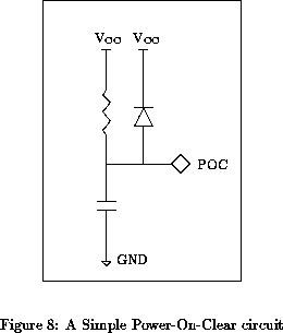
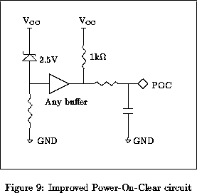
Power-On-Clear is applied to the PCL at the IPOC pin. This is a
Schmitt Trigger input and should be held low for 200mS at power-up. This can be
done using a pull-up resistor, clamp diode to +5V and a capacitor to
ground (Figure 8) but if the +5V rail rises very slowly this
circuit may fail to produce the necessary signal. The improved circuit
(Figure 9) is recommended.
Write CSR#0 is detected within the PCL by gating Write
CSR#0 with the ID30
input.
The Reset Bus condition is detected within the PCL by AND-ing
IBH
and IRBI
. RB must be integrated externally to the PCL to prevent any
short glitch from producing a spurious reset signal. See the FASTBUS
Specification, Section 5.4.2.
Two reset outputs are produced by the PCL: ONCL (Clear) and ONRS (Reset).
ONCL is generated from Power-On-Clear or Reset Bus or Write
CSR#0
. It may be used to clear CSR#0
and CSR#0
. See the FASTBUS Specification, table 8.18
(page 8-15).
ONRS is generated from Power-On-Clear or Write
CSR#0
. It may be used to clear most CSR bits except
CSR#0
and CSR#0
. See the FASTBUS
Specification, table 8.18 (page 8-15).
The reset sources are also used to initialize registers within the
PCL and to clear CSR#7 (Broadcast Class) in the ADIs. This is
automatically performed by the PCL by setting the data multiplexer in the ADIs
to produce zeroes and then loading CSR#7. This procedure is effective
even during a Reset Operation (Write CSR#0
.)