The pinout of the PCL has been optimised to ease PCB layout.
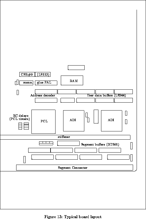
Figure 13 shows a typical layout for a simple slave, having only an
8-bit RAM and a FIFO. CSR#0 for this design uses 74LS112 J-K
flipflops with 74LS244 octal buffers. An optimal design would probably use
PALs with 3-state output.
The FASTBUS specification requires that unused data bits are read as zero;
to meet this requirement this design uses LS244 buffers to drive BD(31:08) low
when reading the RAM. It may be feasible to use 10K pulldown
resistors to bias BD low permanently.