


Next: C Daughterboard
Up: ii Design
Previous: A Physical Construction

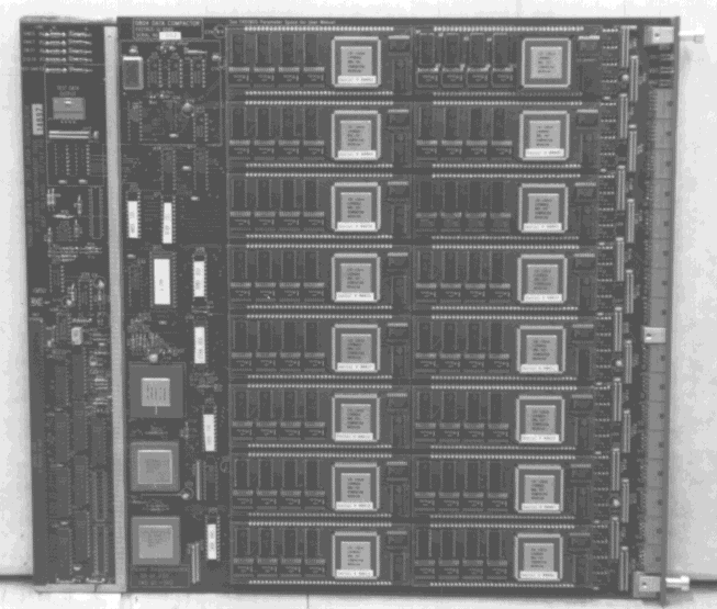
Figure 1 shows the main features of the module.
The FASTBUS Slave Interface consists of the PCL and ADIs, together with the ECL to TTL transceivers. This chip set supports all FASTBUS addressing and data modes and presents a simple TTL interface to the remainder of the board.
The PC board is split into separate powered sections each with its own fuse. A power monitor circuit gives an indication of correct supply voltages in each section by an LED, and also by an error bit in CSR#0 (if the FASTBUS interface is still functional).
A parameter space EPROM is provided, which contains the module serial and asset numbers together with an abbreviated user manual. This information may be read via FASTBUS using standard software.
CCD data is fed in at the front panel, translated to TTL, then presented to the daughterboards. Control information is written to the daughterboards via an internal data bus, which is also used to read out the compacted data.
Channel select logic allows data from each channel to be individually selected, or data from all channels to be read in a single block transfer operation.
An optional Test Data Generator allows synthetic CCD data to be loaded via FASTBUS and routed to any input channel using a test cable.
Next: C Daughterboard
Up: ii Design
Previous: A Physical Construction