


Page 5 shows the daughterboard connections for channels 0 - 3.
Page 6 shows the daughterboard connections for channels 4 - 7.
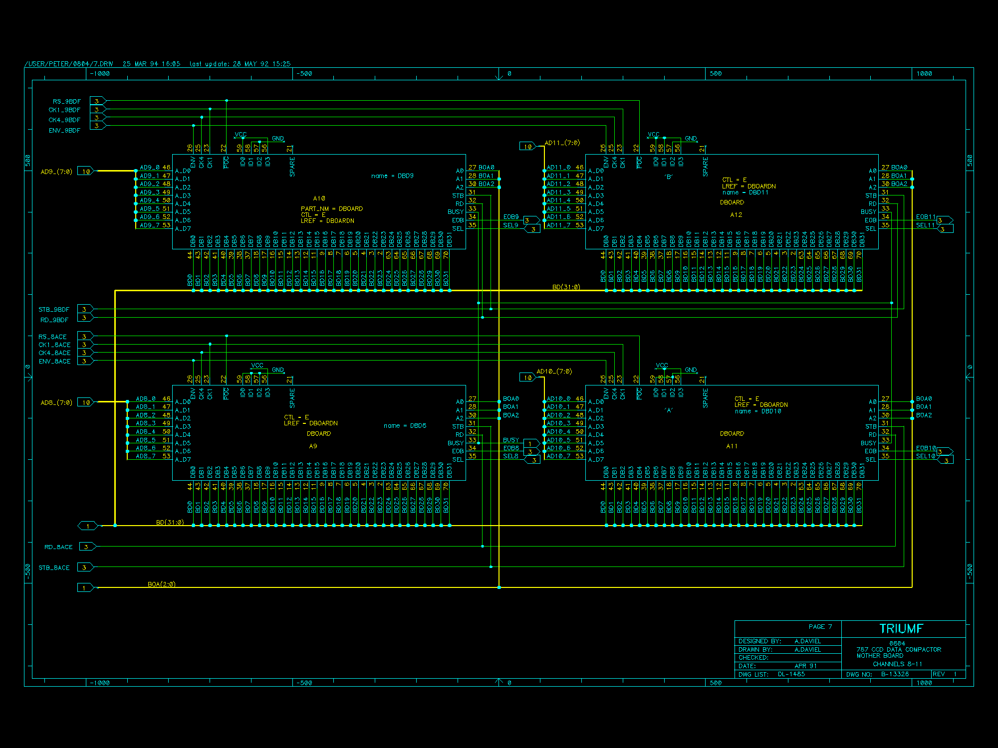
Page 7 shows the daughterboard connections for channels 8 - 11.
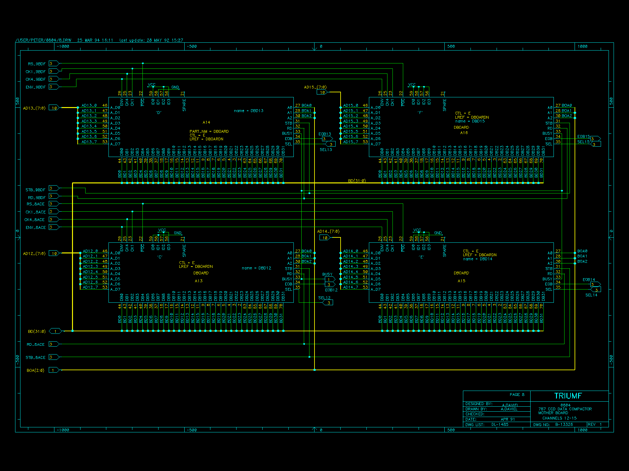
Page 8 shows the daughterboard connections for channels 12 - 15.
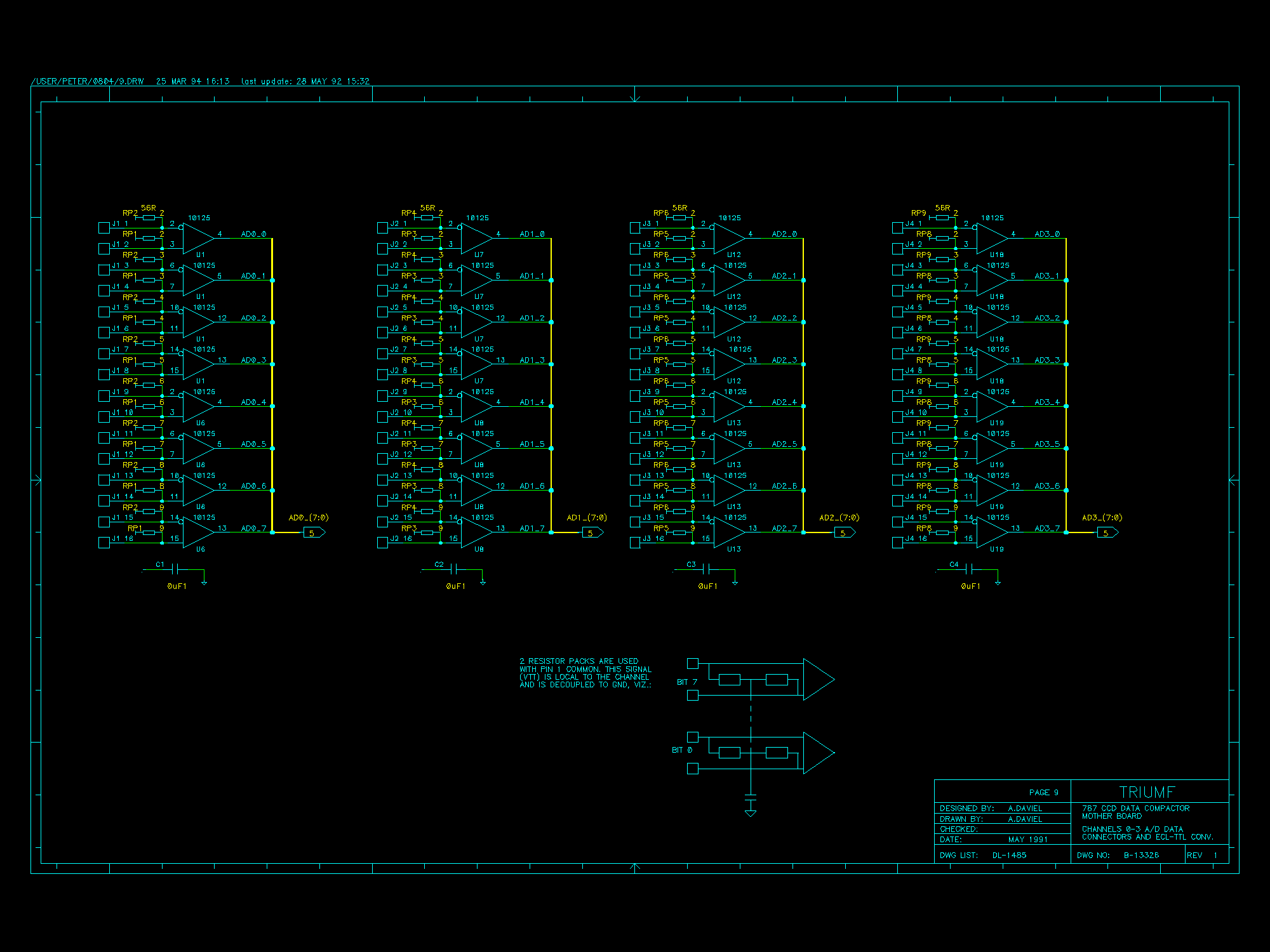
Page 9 shows the input connectors and data buffers for channels 0 - 3.
Page 10 shows the input connectors and data buffers for channels 4 - 7.
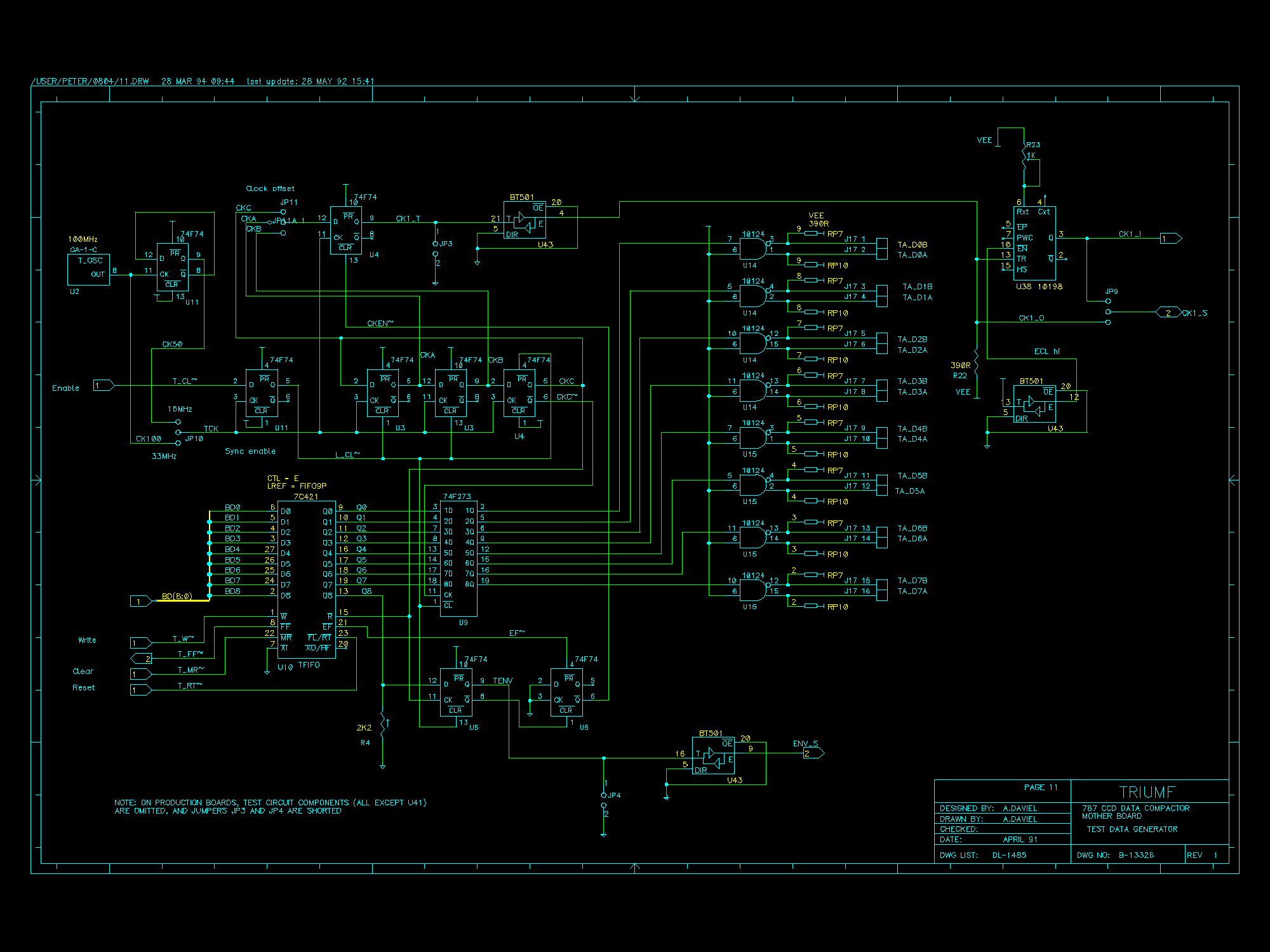
Page 11 shows the optional Test Data Generator.
Page 12 shows the input connectors and data buffers for channels 8 - 11.
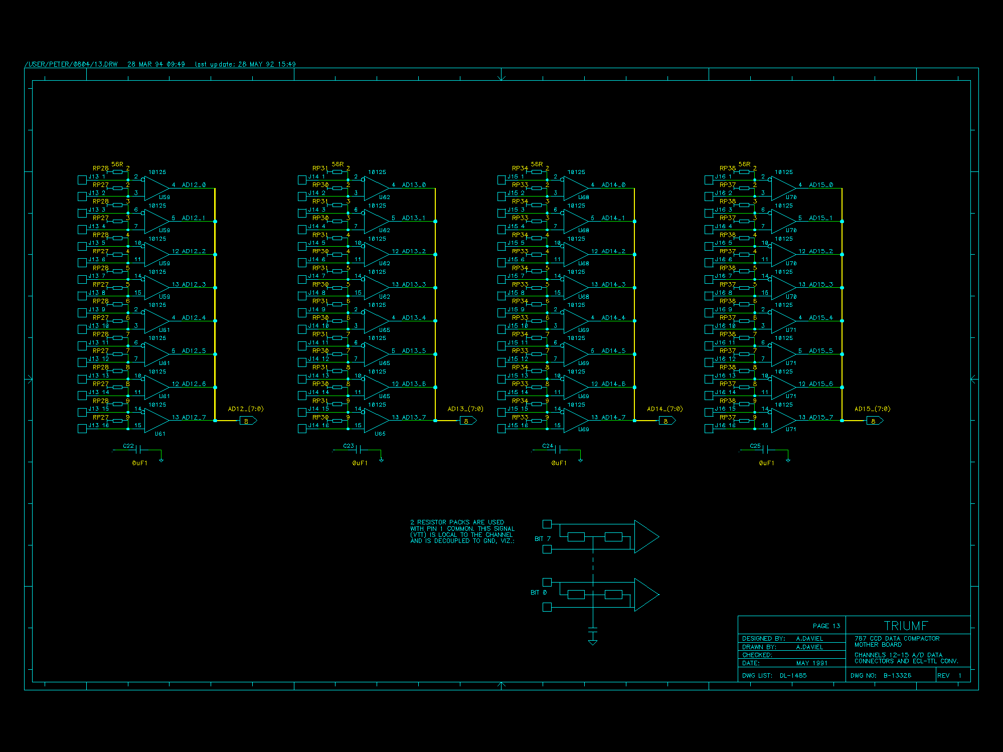
Page 13 shows the input connectors and data buffers for channels 12 - 15.
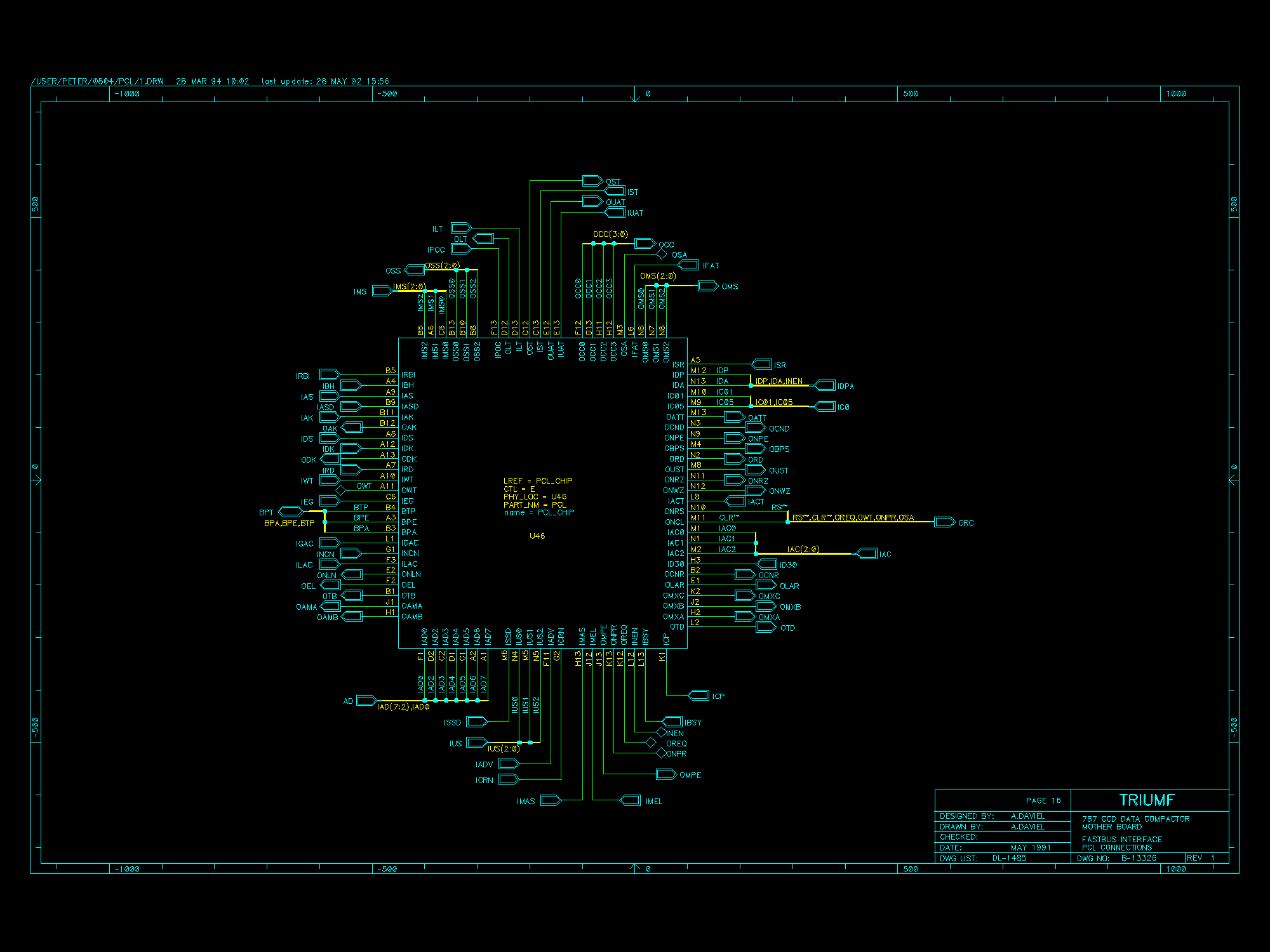
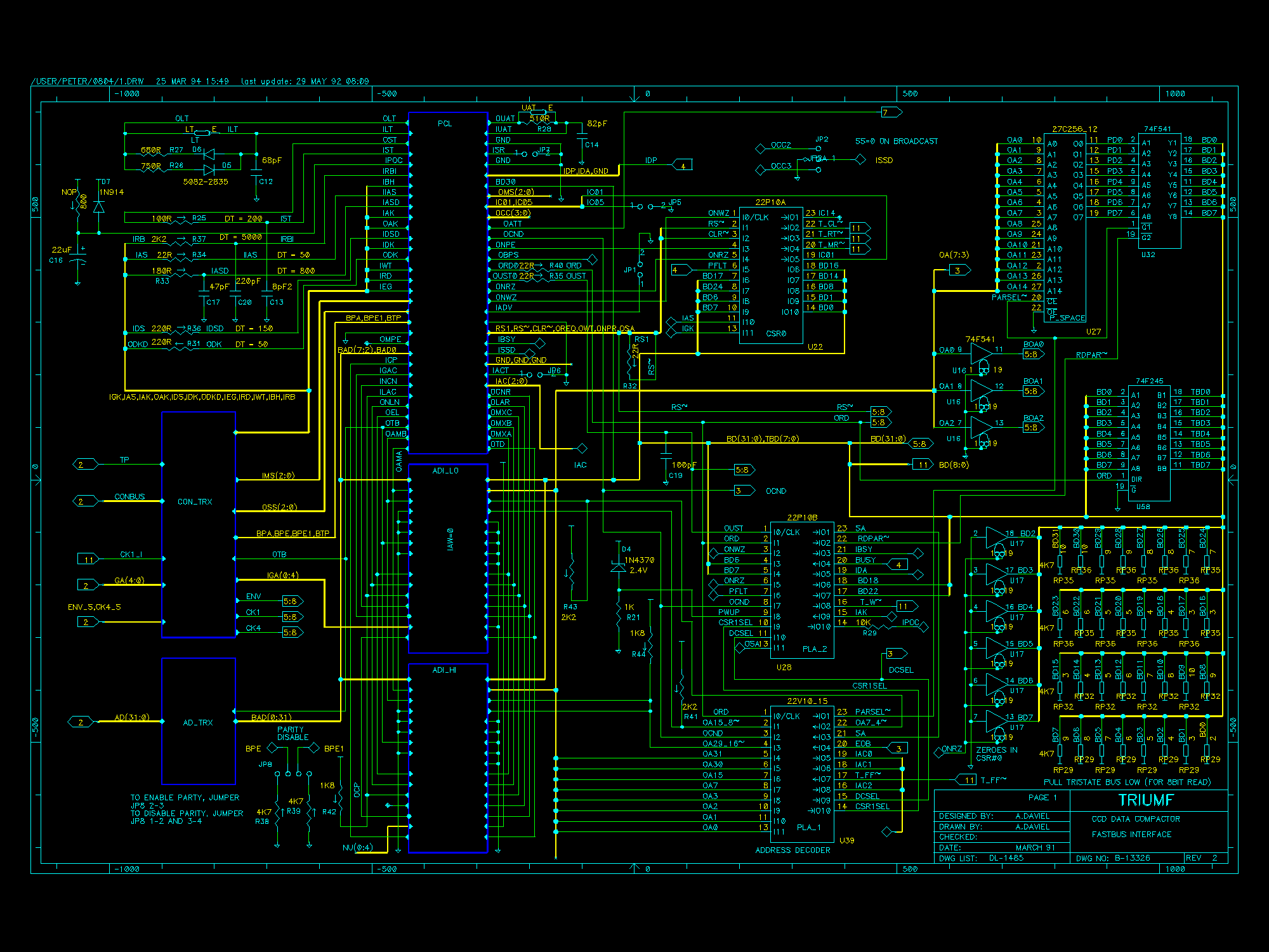
Page pcl/1 shows the individual connections to the PCL gate array.
Page adi_lo/1 shows the individual connections to the lower ADI gate array.
Page adi_hi/1 shows the individual connections to the upper ADI gate array.
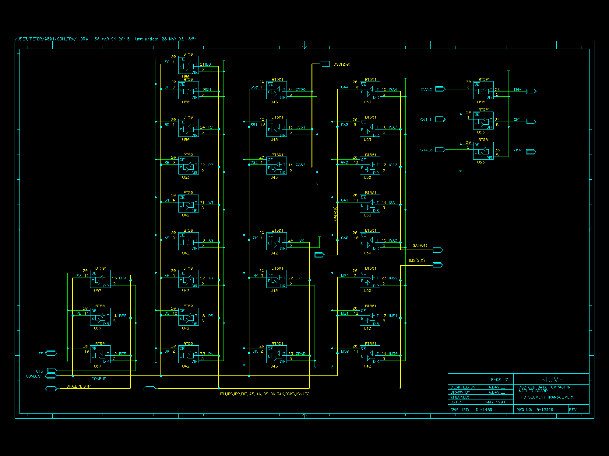
Page con_trx/1 shows the FASTBUS segment signal translators.
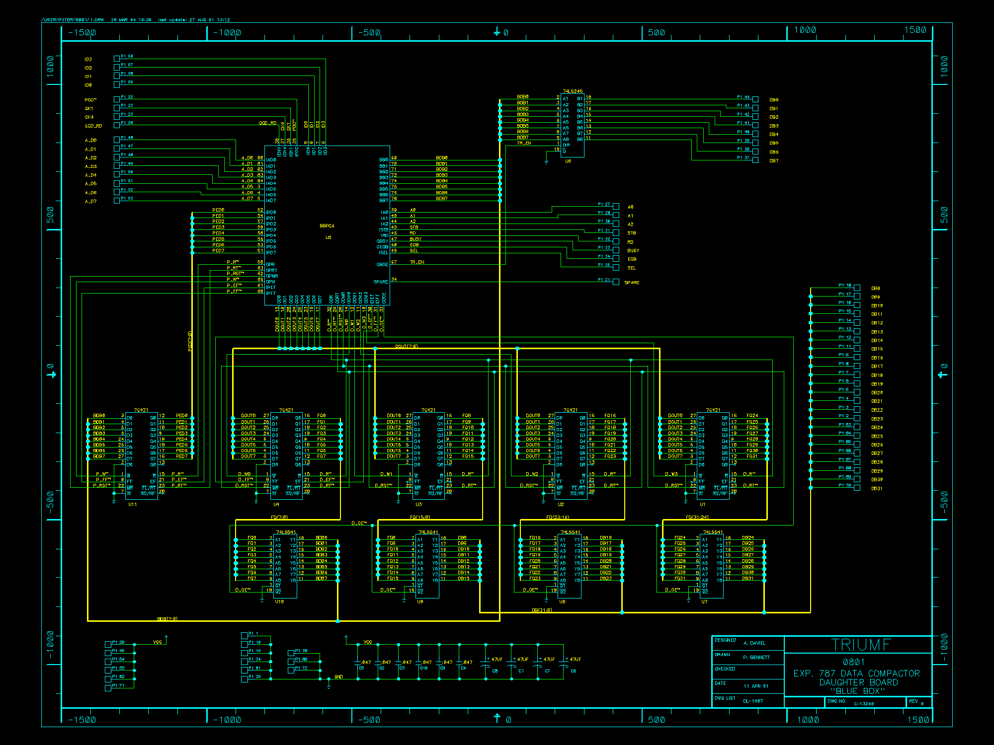
Page db_1 shows the daughterboard logic.
The schematics are also available as compressed HPGL files.
Andrew Daviel